|
|
|
|
|

I'm Online Chat Now
Certification


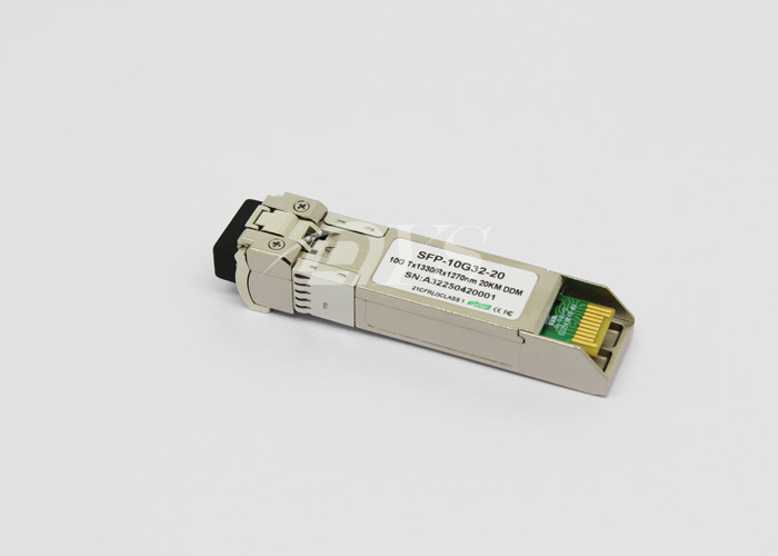
RoHS Compliant 10Gb/s SFP+ Bi-Directional Transceiver, 20km
|
Product Details:
|


Detailed Product Description
RoHS Compliant 10Gb/s SFP+ Bi-Directional Transceiver, 20km Reach
1270/1330nm TX / 1330/1270 nm RX
PRODUCT FEATURES
●Supports 9.95Gb/s to 10.3Gb/s data rates
●Simplex LC Connector Bi-Directional SFP+ Optical Transceiver
●Digital Diagnostic SFF-8472 Compliant
●Hot pluggable
●1:1270nm DFB Laser transmitter,1330nm receiver
2:1330nm DFB Laser transmitter,1270nm receiver
●Up to 20km on 9/125um SMF
●Compliant with IEEE 802.3ae 10GBASE-LR and 10GBASE-LW
●SFP+ MSA SFF-8431 Compliant
●Operating case temperature: 0 to 70 °C
APPLICATIONS
●10GBASE-LR at 10.3125Gbps
●10GBASE-LW at 9.953Gbps
●Other optical links
FUNCTIONAL DIAGRAM
![]()
ABSOLUTE MAXIMUM RATINGS
|
Parameter |
Symbol |
Min. |
Max. |
Unit |
Note |
|
Supply Voltage |
Vcc |
-0.5 |
4.0 |
V |
|
|
Storage Temperature |
|
-40 |
85 |
°C |
|
|
Relative Humidity |
|
|
85 |
% |
|
Note: Stress in excess of the maximum absolute ratings can cause permanent damage to the module
GERERAL OPERATING CHARACTERISTICS
|
Parameter |
Symbol |
Min. |
Typ |
Max. |
Unit |
Note |
|
|
Data Rate |
Ethernet |
|
|
10.3125 |
|
Gb/s |
|
|
Fiber Channel |
|
|
10.518 |
|
|
||
|
Supply Voltage |
Vcc |
3.13 |
3.3 |
3.47 |
V |
|
|
|
Vcc |
|
|
|
V |
|
||
|
Supply Current |
Icc5 |
|
|
|
mA |
|
|
|
Icc3 |
|
|
400 |
mA |
|
||
|
Operating Case Temp. |
Tc |
0 |
|
70 |
°C |
|
|
ELECTRICAL INPUT/OUTPUT CHARACTERISTICS
l Transmitter
|
Parameter |
Symbol |
Min. |
Typ |
Max. |
Unit |
Note |
|
|
Diff. input voltage swing |
|
120 |
|
820 |
mVpp |
1 |
|
|
Tx Disable input |
H |
VIH |
2.0 |
|
Vcc+0.3 |
V |
|
|
L |
VIL |
0 |
|
0.8 |
|||
|
Tx Fault output |
H |
VOH |
2.0 |
|
Vcc+0.3 |
V |
2 |
|
L |
VOL |
0 |
|
0.8 |
|||
|
Input Diff. Impedance |
Zin |
|
100 |
|
Ω |
|
|
l Receiver
|
Parameter |
Symbol |
Min. |
Typ |
Max. |
Unit |
Note |
|
|
Diff. output voltage swing |
|
340 |
650 |
800 |
mVpp |
3 |
|
|
Rx LOS Output |
H |
VOH |
2.0 |
|
Vcc+0.3 |
V |
2 |
|
L |
VOL |
0 |
|
0.8 |
|
||
Note 1) TD+/- are internally AC coupled with 100Ω differential termination inside the module.
Note 2) Tx Fault and Rx LOS are open collector outputs, which should be pulled up with 4.7k to 10kΩ resistors on the host board. Pull up voltage between 2.0V and Vcc+0.3V.
Note 3) RD+/- outputs are internally AC coupled, and should be terminated with 100Ω (differential) at the user SERDES.
OPTICAL CHARACTERISTICS
l Transmitter
|
Parameter |
Symbol |
Min. |
Typ |
Max. |
Unit |
Note |
|
Operating Wavelength |
|
1260 |
1270 |
1280 |
nm |
|
|
1320 |
1330 |
1340 |
||||
|
Ave. output power (Enabled) |
Po |
-3 |
|
3 |
dBm |
1 |
|
Extinction Ratio |
ER |
4.5 |
|
|
dB |
1 |
|
RMS spectral width |
Δλ |
|
|
1 |
nm |
|
|
Rise/Fall time (20%~80%) |
Tr/Tf |
|
|
50 |
ps |
2 |
|
Optical modulation amplitude |
OMA |
-6.2 |
|
|
dBm |
|
|
Dispersion penalty |
|
|
|
1 |
dB |
|
|
Output Optical Eye |
Compliant with IEEE 0802.3ae |
|||||
l Receiver
|
Parameter |
Symbol |
Min. |
Typ |
Max. |
Unit |
Note |
|
Operating Wavelength |
|
1320 |
1330 |
1340 |
nm |
|
|
1260 |
1270 |
1280 |
||||
|
Sensitivity |
Psen |
|
|
-14.4 |
dBm |
3 |
|
Min. overload |
Pimax |
0.5 |
|
|
dBm |
|
|
LOS Assert |
Pa |
-30 |
|
|
dBm |
|
|
LOS De-assert |
Pd |
|
|
-16 |
dBm |
|
|
LOS Hysteresis |
Pd-Pa |
0.5 |
|
4 |
dB |
|
Note 1) Measured at 10.3125b/s with PRBS 231 – 1 NRZ test pattern.
Note 2) 20%~80%
Note 3) Under the ER worst case, measured at 10.3125 Gb/s with PRBS 231 - 1 NRZ test pattern for BER < 1x10-12
PIN DEFINITIONS AND FUNCTIONS
![]()
![]()
|
Pin |
Symbol |
Name/Description |
|
1 |
VEET [1] |
Transmitter Ground
|
|
2 |
Tx_FAULT [2] |
Transmitter Fault
|
|
3 |
Tx_DIS [3] |
Transmitter Disable. Laser output disabled on high or open
|
|
4 |
SDA [2] |
2-wire Serial Interface Data Line |
|
5 |
SCL [2] |
2-wire Serial Interface Clock Line
|
|
6 |
MOD_ABS [4] |
Module Absent. Grounded within the module
|
|
7 |
RS0 [5] |
Rate Select 0 |
|
8 |
RX_LOS [2] |
Loss of Signal indication. Logic 0 indicates normal operation |
|
9 |
RS1 [5] |
Rate Select 1
|
|
10 |
VEER [1] |
Receiver Ground
|
|
11 |
VEER [1] |
Receiver Ground
|
|
12 |
RD- |
Receiver Inverted DATA out. AC Coupled
|
|
13 |
RD+ |
Receiver DATA out. AC Coupled
|
|
14 |
VEER [1] |
Receiver Ground
|
|
15 |
VCCR |
Receiver Power Supply
|
|
16 |
VCCT |
Transmitter Power Supply
|
|
17 |
VEET [1] |
Transmitter Ground
|
|
18 |
TD+ |
Transmitter DATA in. AC Coupled
|
|
19 |
TD- |
Transmitter Inverted DATA in. AC Coupled
|
|
20 |
VEET [1] |
Transmitter Ground
|
Notes:
[1] Module circuit ground is isolated from module chassis ground within the module.
[2].should be pulled up with 4.7k – 10k ohms on host board to a voltage between 3.15Vand 3.6V.
[3]Tx_Disable is an input contact with a 4.7 kΩ to 10 kΩ pullup to VccT inside the module.
[4]Mod_ABS is connected to VeeT or VeeR in the SFP+ module. The host may pull this contact up to Vcc_Host with a resistor in the range 4.7 kΩ to10 kΩ.Mod_ABS is asserted “High” when the SFP+ module is physically absent from a host slot.
[5] RS0 and RS1 are module inputs and are pulled low to VeeT with > 30 kΩ resistors in the module.
TYPICAL INTERFACE CIRCUIT
![]()
Recommended power supply filter
![]()
Note: Inductors with DC resistance of less than 1Ω should be used in order to maintain the required voltage at the SFP input pin with 3.3V supply voltage. When the recommended supply filtering network is used, hot plugging of the SFP transceiver module will result in an inrush current of no more than 30 mA greater than the steady state value
PACKAGE DIMENSIONS
![]()
ORDERING INFORMATION
|
Part Number |
Description |
|
|
DYS-SFP+-WDM-1220 |
SFP+ Plus BiDi,10.3125Gbps,1270nm,20km,0~70℃, with DDM |
|
|
DYS-SFP+-WDM-1320 |
|
Contact Details
China Poly Solar Panel Online Market
Send your inquiry directly to us
More Bi Directional Inverter